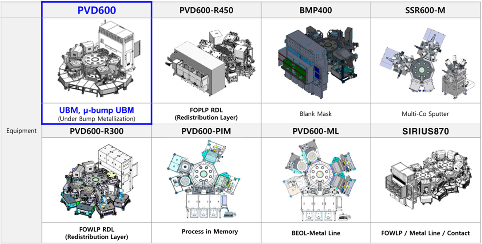

Sputter System (WLP/PLP)
In addition to the ARES™ PVD600 for UBM process, ATST can also provide FoPLP Sputter
equipment and
u-bump Sputter equipment for TSV process, and FoWLP Sputter equipment will be available from 2025.
- The ARES™ PVD600 system is a Sputter equipment for depositing metal films. In the semiconductor packaging process using flip-chip technology, it can perform the UBM (Under Bump Metalization) process for input/output signal transmission of CPB (Cu Pillar Bump) structure.
- It consists of a Multi-Degas chamber (a chamber composed of multiple slots that can perform out-gasing), a CCP-type plasma cleaning chamber (uniformly removes the natural oxide film), and a PVD chamber that deposits metal films (Ti&Cu) in sequence, which can achieve the deposition of high-quality metal films.
- The cavity structure has a long maintenance cycle and fast back-up, which can save maintenance costs. The excellent productivity based on the wafer flow adapted to production and the proven pasting process control contributes to the improvement of customer production capacity.
PVD Line-up